Chapter4_ProcessorFundamentals
Central Processing Unit (CPU) Architecture
Von Neumann model
- Single processor
- Program consists of a sequence of stored instructions
- Instructions and data are indistinguishable
- … are stored in a contiguous block of main memory
- Instructions are fetched and executed in sequence
Stored-program concept
- Program must be resident in main memory to be executed
- Program consists of a sequence of instructions
- Which occupy a contiguous block of main memory
- Instructions and data are indistinguishable
- Each instruction is fetched, decoded, then executed
- Instruction fetch and data operation cannot occur at the same time
Registers
General purpose registers
- Hold data that is frequently used by the CPU
- Can be used by the programmer when addressing the CPU
- e.g. accumulator
Special purpose registers
Have a specific function within the CPU
Hold the program state
PC (Program Counter)
- Stores the address of the next instruction to be fetched
MDR (Memory Data Register)
- Stores the data in transit between memory and other registers
- Holds the instruction before it is passed to the CIR
- The location accessed is what is stored in MAR
MAR (Memory Address Register)
- Stores the address of the memory location which is about to be accessed
ACC (Accumulator)
- Stores the value of calculation by ALU
IX (Index Register)
- Used to carry index addressing operation
CIR (Current Instruction Register)
Stores the current instruction being executed and decoded
Status Register
- Independent bits/flag
- Each flag is set depending on an event
- e.g. overflow, zero, negative, carry flag
ALU (Arithmetic and Logic Unit)
- Carries out arithmetic calculations
- Carries out logic operations
- Holds the result in ACC
CU (Control Unit)
- Sends and receives signals
- Synchronizes operations
- Control the execution of operations
- e.g. input/output
System clock
- Sends out a number of pulses in a given time interval
- Each processor operation takes several cycles to execute
- The higher the clock frequency, the shorter the execution time and the better the performance
IAS (Immediate Access Store)
- Holds all the data and programs that the processor/CPU needs to access
Bus
- Address bus
- Transfer address of memory and input/output position
- Uni-directional
- Data bus
- Carries data between processor and memory
- Bi-directional
- Control bus
- Transmit signals between the control unit
- Dedicated bus since all timing signals are generated according to control signal
- Address bus
Performance factors
- Number of cores
- Each cores processes one instruction per clock pulse
- Multiple cores means that sequence of instructions can be split between them
- … and so more than one instruction is executed per clock pulse
- More cores decreases the time taken to complete task
- Bus width
- Bus width determines the number of bits that can be simultaneously transferred
- Increasing bus width increases the number of bits that can be moved at one time
- … hence improving processing speed as fewer transfers are needed
- e.g. double the width of the data bus moves 2x data per clock pulse
- Clock speed
- Each instruction is executed on a clock pulse
- … so the clock clock speed determines the number of instructions that can be run per second
- The faster the clock speed the more instructions can be run per second
- Cache memory
- Cache memory uses SRAM while main memory uses DRAM
- … so cache memory is faster than main memory
- Cache memory stores frequently used instructions and data
- When CPU reads memory, it first checks out cache and then moves on to main memory if the required data is not in cache memory
- So this improve processor performance
- Number of cores
Ports
- USB (Universal Serial Bus)
- An asynchronous serial data transmission method
- The computer automatically detects that a device is present (due to a small change in the voltage level)
- The device is automatically recognized, and the appropriate device driver is loaded up
- If a new device is detected, the computer will look for the device driver which matches the device. If this is not available, the user is prompted to download the appropriate software
- HDMI (High Definition Multimedia Interface)
- The computer automatically detects that a device is present (due to a small change in the voltage level)
- Handshake between the display and the computer
- The display sends meta data about itself (resolution, color depth, etc.)
- VGA (Video Graphics Array)
- The computer automatically detects that a device is present (due to a small change in the voltage level)
- Handshake between the display and the computer
- The display sends meta data about itself (resolution, color depth, etc.)
- USB (Universal Serial Bus)
F-E (Fetch-Execute) cycle
- Fetch
- The next instruction is fetched from the memory address in PC
- This instruction in stored in CIR
- The PC is incremented by 1
- The instruction is decoded
- Execute
- The processor passes the decoded instruction as a set of control signals to the appropriate components within the computer system
In register transfer notation:
- $\text{MAR} ← [\text{PC}]$ contents of PC copied into MAR
- $\text{PC} ← [\text{PC}] + 1$ PC is incremented by 1
- $\text{MDR} ← [[\text{MAR}]]$ data stored at address shown in MAR is copied into MDR
- $\text{CIR} ← [\text{MDR}]$ contents of MDR copied into CIR
- Fetch
Interrupts
- At the start oof each F-E cycle the processor checks for interrupts
- Check if an interrupt flag is set in status register
- Processor identifies source of interrupt
- Processor checks priority of interrupt
- If interrupt priority is high enough
- Processor saves current contents of registers
- Processor calls ISR (Interrupt Service Routine)
- Address of ISR is loaded into PC
- When servicing of interrupt complete, processor restores registers
- Processor continues with next F-E cycle
Assembly Language
Two-pass assembler
- Pass 1
- Read the assembly language program one line at a time
- Ignore anything not required, such as comments
- Allocate a memory address for the line of code
- Check the opcode is in the instruction set
- Add any new labels to the symbol table with the address, if known
- Place address of labelled instruction in the symbol table
- Pass 2
- Read the assembly language program one line at a time
- Generate object code, including opcode and operand , from the symbol table generated in Pass 1
- Save or execute the program
- Pass 1
Groups of instructions
Data movement
- Allow data stored at one location to be copied into the accumulator
Opcode Operand Explanation LDM #n Immediate addressing. Load the number to ACC LDD Direct addressing. Load the contents of the location at the given address to ACC LDI Indirect addressing. The address to be used is at the given address. Load the contents of this second address to ACC LDX Indexed addressing. Form the address from + the contents of the index register. Copy the contents of this calculated address to ACC LDR #n Immediate addressing. Load the number n to IX MOV Move the contents of the accumulator to the given register STO Store the contents of ACC at the given address Input and output of data
- These instructions allow data to be read from the keyboard or output to the screen
Opcode Operand Explanation IN Key in a character and store its ASCII value in ACC OUT Output to the screen the character whose ASCII value is stored in ACC Arithmetic operations
- These instructions perform simple calculations on data stored in the accumulator and store the answer in the accumulator, overwriting the original data
Opcode Operand Explanation ADD Add the contents of the given address to the ACC ADD #n / Bn / &n Add the number n to the ACC SUB Subtract the contents of the given address from the ACC SUB #n / Bn / &n Subtract the number n from the ACC INC Add 1 to the contents of the register (ACC or IX) DEC Subtract 1 from the contents of the register (ACC or IX) PS: #n means that n is in denary, Bn means that n is in binary, &n means that n is in hexadecimal
Unconditional and conditional instructions
Opcode Operand Explanation JMP Jump to the given address JPE Following a compare instruction, jump to if the compare was True JPN Following a compare instruction, jump to if the compare was False Compare instructions
Opcode Operand Explanation CMP Compare the contents of ACC with the contents of CMP #n Compare the contents of ACC with number n CMI Indirect addressing. The address to be used is at the given address. Compare the contents of ACC with the contents of this second address
Addressing modes
Immediate addressing
The value of the operand is used
Direct addressing
The contents of the location in the given address is used
Indirect addressing
The address is the content of the given address
Indexed addressing
The address is formed by adding the given address by the contents in the Index Register
Relative addressing
The address is formed by adding the current address by the operand
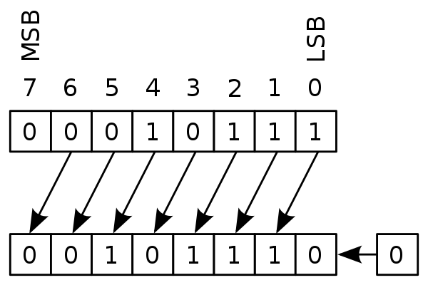
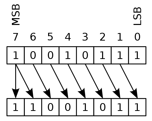
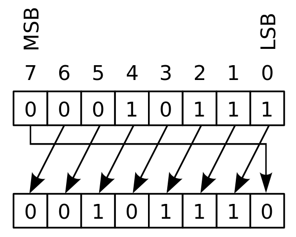
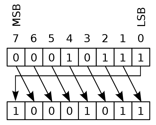
Bit manipulation
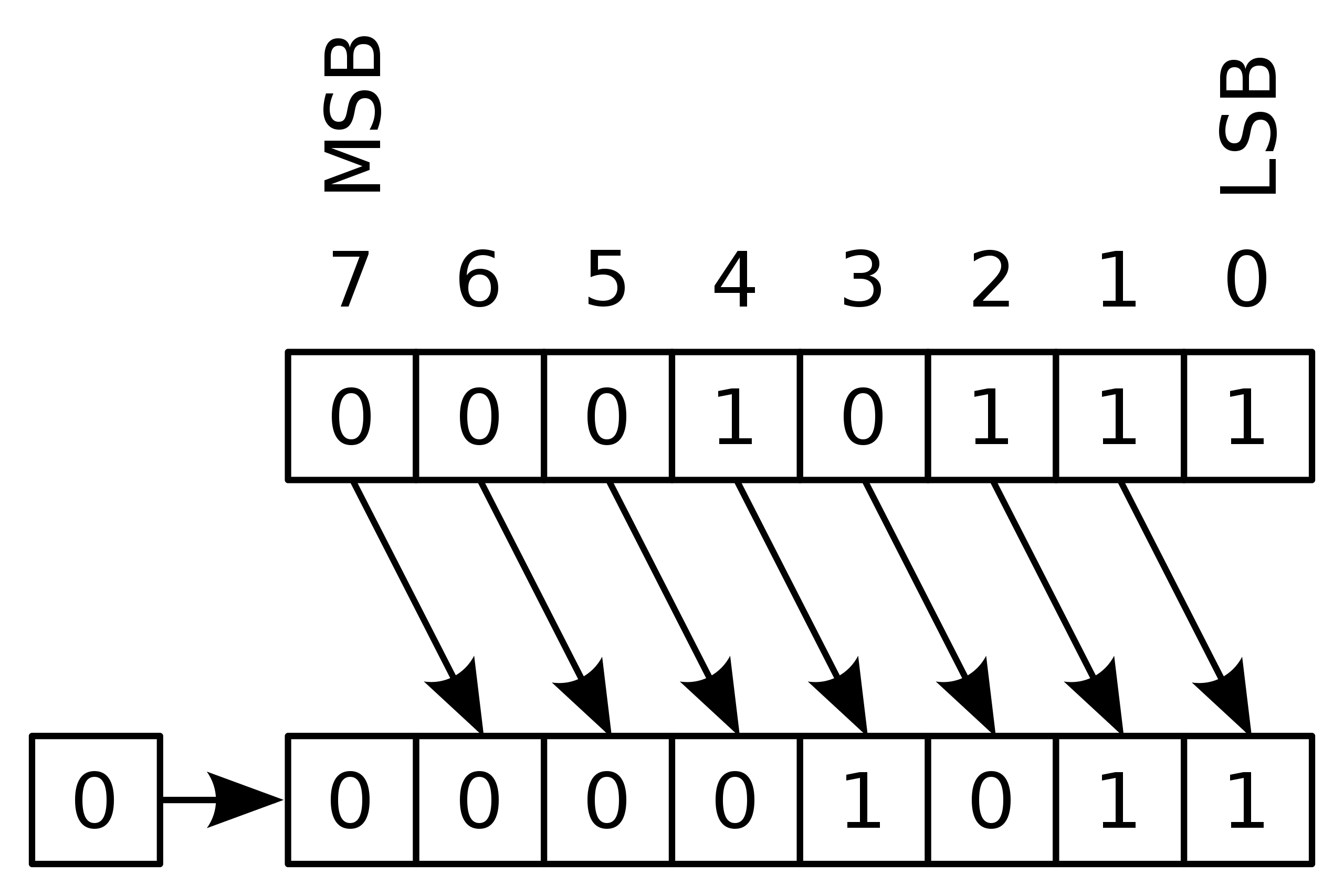
Binary shifts
Logical shift
Left shift:

Right shift:
Arithmetic shift
Left shift:
Right shift: (The empty position in the most significant bit is filled with a copy of the original MSB)
Cyclic shift
Left shift:
Right shift:
How bit manipulation is used to monitor/control a device
- Each bit in a register or memory location can be used as a flag and would need to be tested, set or cleared separately (bit masking)
- AND is used to check if the bit has been set
- OR is used to set the bit
- XOR is used to clear a bit that has been set