Chapter15.2: Boolean Algebra And Logic Circuits

Adders➕
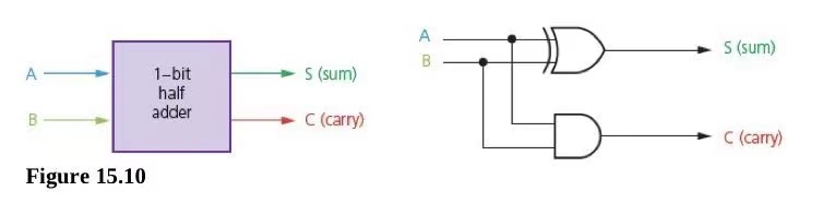
Half adder
Carries out binary addition on 2 bits generating two outputs
- The sum bit
S - The carry bit
C
| Input | Output | ||
|---|---|---|---|
| A | B | S | C |
| 0 | 0 | 0 | 0 |
| 0 | 1 | 1 | 0 |
| 1 | 0 | 1 | 0 |
| 1 | 1 | 0 | 1 |
Full adder
The half adder is unable to deal with the addition of several binary bits (e.g. an 8-bit byte). To enable this, we have considered the full adder circuit
| Inputs | Outputs | |||
|---|---|---|---|---|
| A | B | C |
S | C |
| 0 | 0 | 0 | 0 | 0 |
| 0 | 0 | 1 | 1 | 0 |
| 0 | 1 | 0 | 1 | 0 |
| 0 | 1 | 1 | 0 | 1 |
| 1 | 0 | 0 | 1 | 0 |
| 1 | 0 | 1 | 0 | 1 |
| 1 | 1 | 0 | 0 | 1 |
| 1 | 1 | 1 | 1 | 1 |

Flip-flop
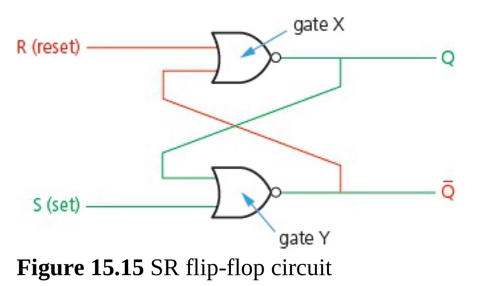
SR Flip-flop
The SR flip-flop or
latchis a simple example of a sequential circuit. It can be constructed with two NAND gates or two NOR gates.
The properties of SR flip-flop explained why it can be used as a storage device for 1 bit and therefore could be used as a component in RAM because a value is stored but can be altered.
The alternative NAND gate circuit for the SR flip-flop has a similar structure but the labelling is different. The important difference is that setting is achieved when S=0 & R=1 and resetting with R=0 and S=1.
NOR gates implementation
NAND gate implementation


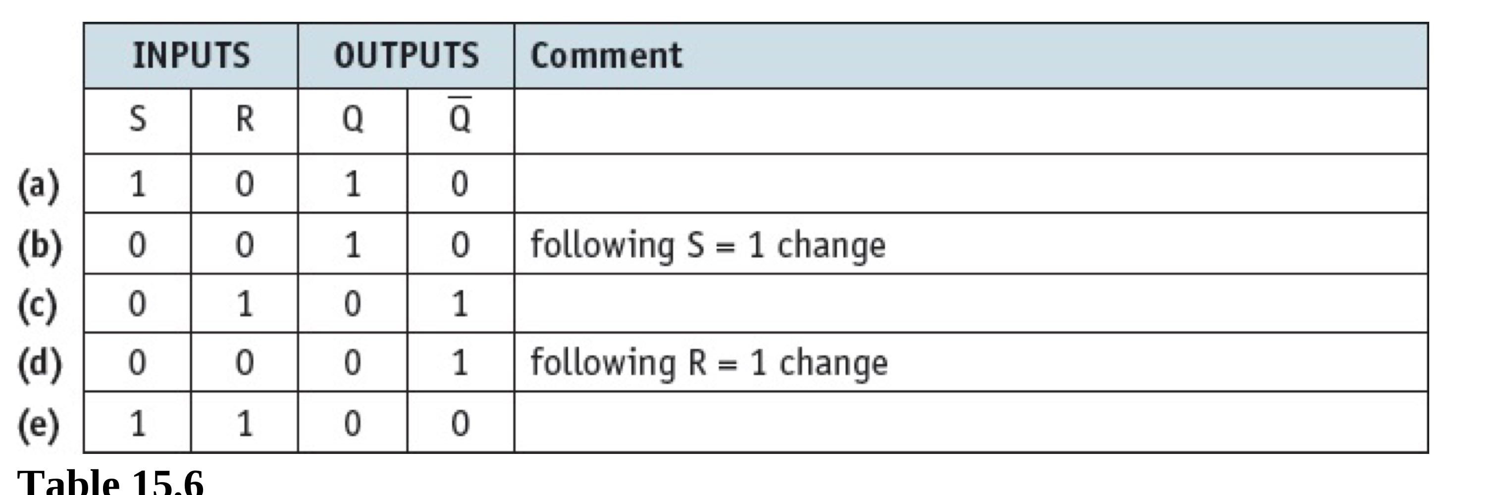
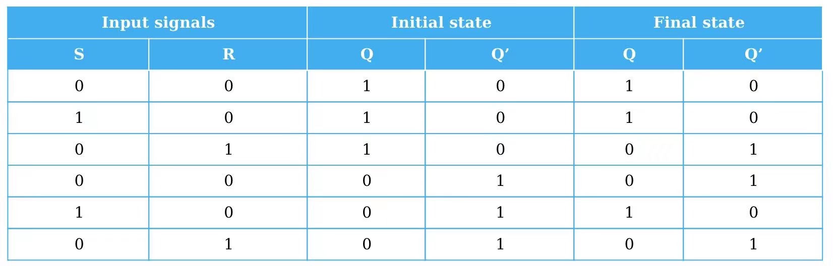
Why is the final row a problem?
- Q and not Q have the same value
- Q and not Q should be the complement to each other
- Flip-flop becomes unstable
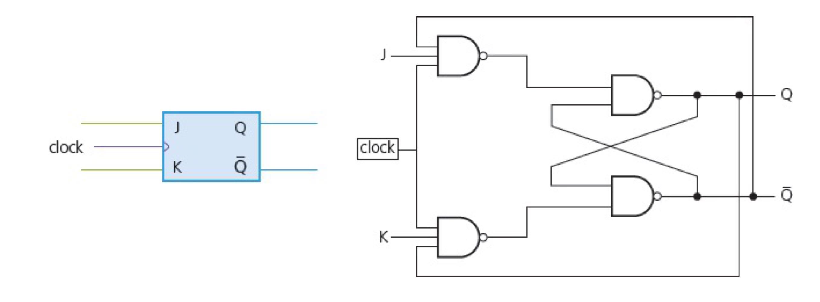
JK Flip-flop
In addition to the possibility of entering an invalid state there is also the potential for a circuit to arrive in an uncertain state if inputs do not arrive quite at the same time. In order to prevent this, a circuit may include a clock pulse input to give a better chance of synchronising inputs. The JK flip-flop is an example.

Past-paper questions
Why JK flip-flop is an improvement to the SR flip-flop
- The SR flip-flop has an invalid combination of SR which allows Q and not Q to have the same value
- The JK flip-flop does not allow Q and not Q to have the same value
Advantages of JK flip-flop
- All four possibilities are valid
- The 1-1 combination changes to output to logical complement
- Unstable state avoided
- Invalid state cannot occur
Explain the role of flip-flop in a computer
- A flip flop can be stored either a 1 or 0
- Computers use bits to store data
- Flip flop can therefore be used to store bits
- Memory can be created from flip-flop
Describe the role of flip-flop in a computer:
- Circuit / electrical components(construction)
- With two states
- Used for data storage elements // memory
- … to store 1 bit of data
Difference between SR flip-flop and JK flip-flop
- SR flip-flop has a undefined/invalid/intermediate state // JK flip-flop is stable
- for a SR flip-flop constructed using two NOR gates, when S=1 and R=1. The Q and not Q will be both 0. This is invalid since Q and not Q should be the logical complement to each other.
- JK flip-flop has a clock pulse to synchronize input

Boolean Algebra

K-map
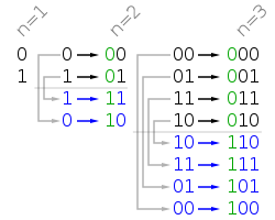
Grey code